 Advanced packaging technology for AI and power semiconductors
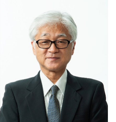
Prof. Katsuaki Suganuma
Osaka University, Japan
Abstract:
Advanced packaging technology for AI
and power semiconductors
Prof. Katsuaki Suganuma, Osaka University, Japan
Packaging materials and processes with basic science has been intensively focused by many
researchers and engineers in the world. These factors are the keys for us to explore new
technology both for AI semiconductors and for WBG semiconductors. The superior functions
of these semiconductors can be retrieved by basic science supporting device structures,
especially materials combination and bonded interfaces. One of the examples will be shown as
the nano voids issue for substrates. The weakness of built up substrates often causes serious
failure incident in the market for many years. The most serious failure occurs at the microvias,
which is sometimes called as “weak micro-via”. Macroscopic observation of via bottom have
been carried out by SEM and TEM by researchers. Nevertheless, root cause has not been yet
understood until recently since nano voids are really in single nano size and no effective
analytical method has been applied. Our group has carried out nano analysis by high resolution
TEM and atom probe tomography with XPS on the nano voids and then, finally discovered the
presence of substantial residues in the electroless Cu layer in via bottom of substrates. Followed
by this finding, the removal of the residues can suppress the nano voids formation at via bottom.
This modification in electroless Cu plating can improve the reliability of substrates. Thus, basic
science providing new information on hetero-interfaces in semiconductors can open the
effective ways to the reliable and excellent functions for advanced edge AI / WBG power
semiconductors.
Speaker's Biography:
He received the degree of Dr. Engineer from Tohoku University in 1982. He became a research
assistant of ISIR (Institute of Scientific and Industrial Research), Osaka University in 1982, an
associate professor of National Defense Academy in 1986, and a professor of ISIR of Osaka
University in 1996. He was the director of Nanotechnology Center of ISIR in 2007-2009, the
director of ISIR in 2018-2020. He is currently Specially Appointed Professor and Professor
Emeritus of Osaka University, Executive Advisor of Daicel Corp., Managing Director of Izumi
Science. He has worked on lead-free soldering, conductive adhesive, power electronics
packaging and printed electronics. He published about 450 journal papers, 160 reviews and
many books on packaging technology such as “Wide Bandgap Power Semiconductor
Packaging”. He is currently in charge of IEC SC47D Semiconductor Packaging Japan
Committee/JEITA, of Advanced Semiconductor Task Force/JEITA, and of Standardization of
Thermal Property Evaluation of WBG Power Devices/JFCA.