Fine Pitch Thermo Compression Bonding with Focus on No Flux Bonding
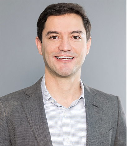
Dr. Thiago Moura
Advanced Packaging Process Manager, Besi Austria
Abstract:
As the industry moves to higher density interconnects driven by artificial intelligence (AI) and machine learning a need for multiple interconnect technologies arises. Whilst Hybrid bonding (HB) is addressing 9µm pitches and below in high volume manufacturing (HVM), thermo compression bonding (TCB) is still a viable candidate for <25µm pitch applications. However, issues arise as the copper pillars move closer to each other, such as solder bridging during bonding if solder is squeezed out or opens if warpage is not controlled or heat application is not homogeneously applied. A further topic is how to remove flux residues from such a small gap between die and substrate (<8µm) and with such high copper pillar density. As such fluxless TCB is seen as an enabler for sub 25µm TCB.
This presentation outlines the designs implemented in a die bonder to achieve such a scenario, whilst highlighting state of the art gas consumption values, which are a big impact on return on investment. A comparison of several methods that can achieve fluxless bonding will also be showcased. The tool layout will show that the substrate and uplooking cameras are placed inside the heated controlled atmosphere to ensure maximum accuracy and no impact to the material from exposure to outside atmosphere. The bonding tools and auto change mechanism are also placed inside the controlled atmosphere allowing for heterogeneous integration to be carried out seamlessly.
Accuracy and planarity are also showcased through several cross sections to achieve sub-micron accuracy. The test vehicle in question also posed particular challenges due to its multi pitch nature where 20µm, 10µm, 7µm and 5µm pitches are present, testing the limits of TCB. Electrical testing results via daisy chain to assess joint reliability are presented.
Speaker's Biography:
Thiago has a PhD in Electrical Engineering Microelectronics, a Masters in Material Engineering, and an Undergraduation in Physics. He has over 10 years of packaging experience in the semiconductor industry. Before joining BESI, Thiago worked with surface engineering, plasma engineering and packaging technology at different applied research institutes. He then joined BESI Singapore in 2016, moving to Besi Austria in 2019 as senior process specialist and currently occupies the role of Advanced Packaging Process Manager. His work at Besi has taken him all over the world working onsite with customers to solve problems, implement and improve processes.