Advanced Substrates for Chiplets, Heterogeneous Integration, and Co-Packaged Optics
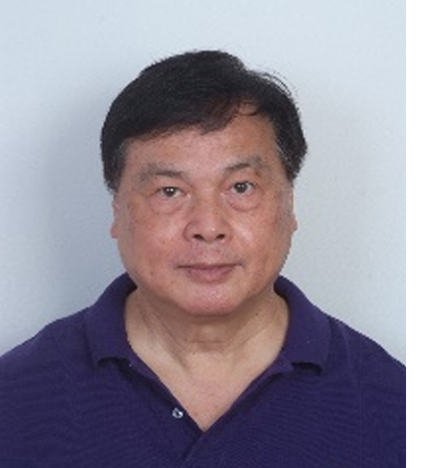
Dr. John H. LAU
Unimicron Technology Corporation, Taiwan, China
Abstract:
Today, most of the package substrates for HPC driven by AI (artificial intelligence) are made by the 2.5D IC integration. In general, for 2.5D or CoWoS (chip on wafer on substrate), the SoC and high bandwidth memories (HBMs) are supported by a TSV-interposer and then solder bump and underfill on a build-up package substrate. However, because of the ever-increasing size of the TSV-interposer, the manufacture yield loss of the TSV-interposer is becoming unbearable. The key players such as NVIDIA, AMD, Intel, SK Hynix, Samsung, Micron, TSMC, etc. are working very hard to eliminate the TSV interposer and put the HBMs directly on top of the SoC (3.3D IC integration). Front-end integration of some of the chiplets (before package heterogeneous integration) can yield a smaller package size and a better performance (3.5D IC integration). In the past few years, 2.3D IC integration or CoWoS-R is getting lots of traction. The motivation is to replace the TSV-interposer with a fan out fine metal L/S redistribution-layer (RDL)-substrate (or organic-interposer). In general, for 2.3D, the package substrate structure (hybrid substrate) consists of a build-up package substrate, solder joints with underfill, and the organic-interposer. Today, 2.3D is already in production. Recently, TSMC published two papers on replacing the large-size TSV-interposer by LSIs (local silicon interconnects, i.e. Si bridges) and embedding the LSIs in fan-out RDL-substrate. TSMC called it CoWoS-L. Recently, since Intel’s announcement on the glass core substrate for their one-trillion transistors to be shipped before 2030, glass core substrate has been a very hot topic. Since the shipments of co-packaged optics (CPO) by Intel and Broadcom CPO have been getting lots of tractions. In this lecture, the introduction, recent advances, and trends in the substrates of 3.5D IC integration, 3.3D IC integration, 3D IC integration, 2.5D IC integration, 2.3D IC integration, 2.1D IC integration, 2D IC integration, fan-out RDL, embedded Si-bridge, CoWoS-R, CoWoS-L, CPO, and glass core for HPC driven by AI will be discussed. Some recommendations will be provided.
Outline:
1. Introduction
2. Substrate Definition
3. Substrates for Chiplet and Heterogeneous Integration
4. 2D IC Integration
5. 2.1D IC Integration
6. 2.3D IC Integration
7. 2.5D IC Integration
8. 3D IC Integration
9. 3.3D IC Integration
10. 3.5D IC Integration
11. Bridges Embedded in Build-up Substrates
12. Bridges Embedded in Fan-Out EMC with RDLs
13. Glass-Core Build-up Substrates and TGV-Interposers
14. CPO Substrates
15. Summary and Recommendations
Who Should Attend:
If you (students, engineers, and managers) are involved with any aspect of the electronics industry, you should attend this course. It is equally suited for R&D professionals and scientists. The lectures are based on the publications by many distinguish authors and the books (by the lecturer).
Lecturer Biography:
John H Lau, with more than 40 years of R&D and manufacturing experience in semiconductor packaging, has published more than 535 peer-reviewed papers (385 are the principal investigator), 52 issued and pending US patents (31 are the principal inventor), and 24 textbooks. John is an elected IEEE fellow, IMAPS Fellow, and ASME Fellow and has been actively participating in industry/academy/society meetings/conferences to contribute, learn, and share.