Packaging of MEMS and More
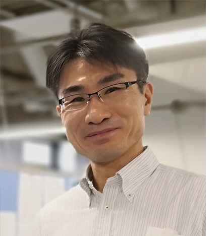
Prof. Shuji Tanaka
Department of Robotics, Graduate School of Engineering, Tohoku University, Japan
Abstract:
This lecture provides an overview of packaging technologies for MEMS, acoustic wave filters, and related devices. Packaging typically involves two levels: (1) wafer-level packaging and (2) plastic molding.
Wafer-level packaging encapsulates devices directly on the wafer using techniques such as wafer bonding and film deposition. This process often achieves hermetic, and sometimes vacuum, sealing of the devices. Electrical connections to the outside of the package are made through lateral feedthroughs or vias. The lecture introduces both historical and modern methods of wafer-level packaging, along with key technologies such as wafer bonding, electrical feedthroughs, and hermeticity evaluation.
Following wafer-level packaging, the second level of packaging involves plastic molding. This includes processes such as wafer dicing, die bonding, wire bonding, plastic molding, and final dicing. For high-frequency devices, flip-chip bonding is increasingly used in place of die and wire bonding. The lecture reviews each of these steps and discusses problems associated with second-level packaging.
Finally, the lecture connects these traditional packaging approaches to emerging advanced packaging technologies used in AI semiconductors. The content is presented from a practical point of view.
Outline:
1. Purpose and outline of packaging
2. Various wafer-level packaging methods
3. Wafer bonding
4. Electrical feedthrough
5. Hermetic test
6. Second level packaging methods
7. Dicing
8. Die bonding, wire bonding and flip chip bonding
9. Plastic molding
10. Advanced packaging
Who Should Attend:
Engineers, designers, researchers, salespersons, and managers in MEMS and semiconductor industry as well as undergraduates and graduate students studying MEMS or semiconductor devices.
Lecturer Biography:
Shuji Tanaka holds a B.E., M.E., and Dr.E. degrees in mechanical engineering from The University of Tokyo, completing his studies in 1994, 1996, and 1999, respectively. He began his professional journey as a Research Associate at Department of Mechatronics and Precision Engineering, Tohoku University in 1999. Subsequently, he assumed the role of Assistant Professor until 2003, followed by Associate Professor at Department of Nanomechanics until 2013. Currently, he holds the position of Professor at Department of Robotics and Microsystem Integration Center, Tohoku University. Additionally, he served as a Fellow of Center for Research and Development Strategy, Japan Science and Technology Agency (JST) between 2004 and 2006, later becoming a Selected Fellow from 2006 to 2018.
He has played key roles in various conferences, notably serving as General Chair of IEEE NEMS 2016, General Co-Chair of IEEE MEMS 2022, Executive Program Chair of Transducers 2023, and General Chair of annual MEMS Engineer Forum since 2019. Additionally, he has been President of Micro-Nano Science and Technology Division, The Japan Society of Mechanical Engineers (JSME) and AdCom member of IEEE Ultrasonics, Ferroelectrics, and Frequency Control Society (UFFC-S). His continuous contributions to the field have earned him the distinction of being an IEEE Fellow and a JSME Fellow.
Shuji Tanaka’s research interests span diverse areas, including MEMS, acoustic wave devices, wafer-level packaging and integration, and piezoelectric devices and materials.